Progress Report for Aden Koperczak
WEEK: 13
Date: 11/17/2023Total hours: 115 hours
Project Hours Since Last Report: 10 hours
Cumulative Semester Project Hours: 115 hours
Description of Individual Project Work Efforts: Improved Game Logic, Made Cables, Helped with Construction, Began Wiring
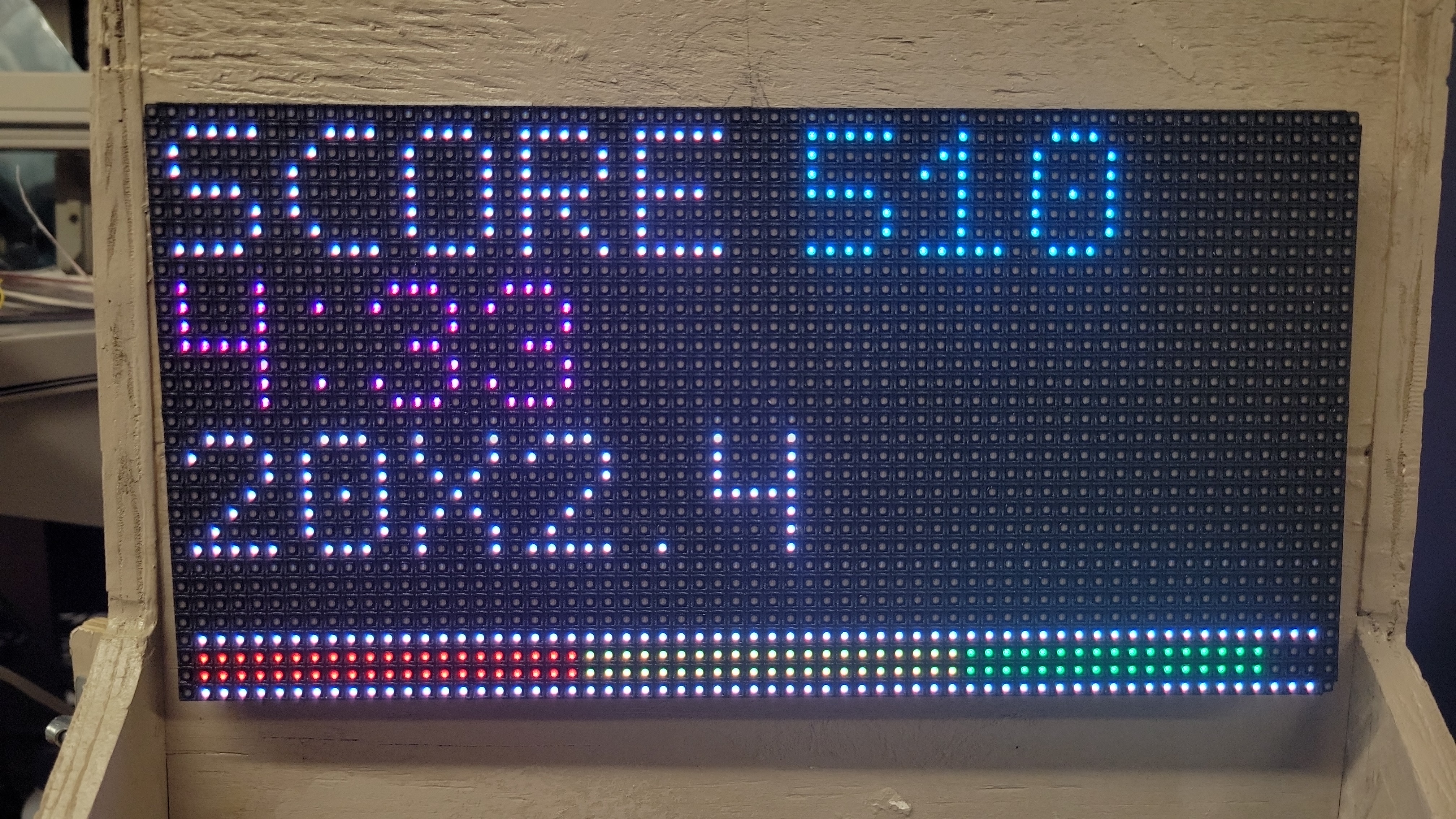
This week I spent around 4 hours working on game logic and the game UI. I started by implementing Combo Mode which took about an hour. Then I worked on improving the UI. This included coloring the text so it was easier to tell what is what when it is displaying a score and time excreta. I also game each game mode which will be useful in labeling and makes navigation more intuitive. I also added the game mode to the conformation text. Finally I experimented with the combo mode display, trying to find a good way to display the multiplier and which combo you have. I settled on the display format in Figure 27. I also added some basic sound normal game mode, although this is likely to change. This brings our UI closer to a final state.
I also spent around 3 hours making cables for the display's power and for the 5 sensors we need. First we measured the needed for the cables and cut the wire. For the displays power cable and one end of the sensor cables we used JST connectors, and had bought some pre terminated ends, so I simple soldered the wire to the pre terminated wire. On the other side of the sensor cables we used a simple pin header so I just had to solder on to those. We also added hear shrink over the solder joints. Finally, I worked the wires so they would be somewhat strait. Overall, I did the power cable on my own, and Htet helped me measure and cut the sensor wires, and did all of the heat shrink for the sensors. I did all of the soldering. This is a key component of our design.
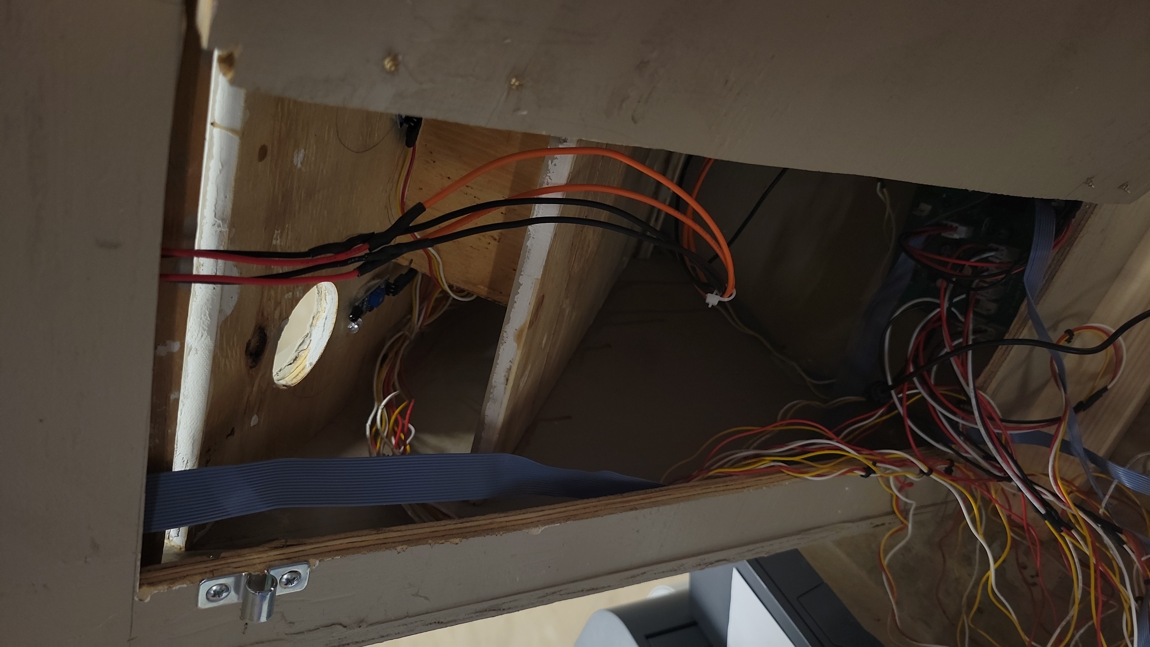
Jinrea and I spent around 2 hours discussing the design of the packaging and getting it ready to be glued. This involved drilling some holes for wires to go through and adding a door to the back of it so we can easily access the wiring. This took a bit more time then I would have expected, but that is likely down our inexperience with this type of work. I have more experience assisting people working with would, and less with doing it myself. This made gluing our machine together much easier.
Finally I spent around an hour working out the cable routing for our machine. This goes in part with the last section, although I did most of this with Htet instead of Jinrea. This included adding clips to attach the wires to so they are not just hanging in the machine. Once they glued it together I put all of the wiring into place as well. Now we have a mostly wired machine. It still needs some cable management but it is a good start.
Progress Report for Aden Koperczak
WEEK: 12
Date: 11/10/2023Total hours: 105 hours
Project Hours Since Last Report: 9 hours
Cumulative Semester Project Hours: 105 hours
Description of Individual Project Work Efforts: Finnish Circuit, Keypad Work, and Began Game Logic.
This week I started by fixing a few issues with our circuit board. In particular we had an issue with our buck starting, and an issue with our some of the pins on our microcontroller where low resistance and interfering with one another. The issue with the buck came down to us not pulling the ON/*OFF pin high. According to the datasheet that should not be an issue but having pulled it up, it works much more consistently. The issue with the micro came down to having flux and isopropyl alcohol under the pins. This was solved by blowing out under the microcontroller. To be clear, we had already done that, and ended up doing it three or four times before it worked. Eric helped me with this as well. Together this took around 3 hours. This has made our board work more consistently.
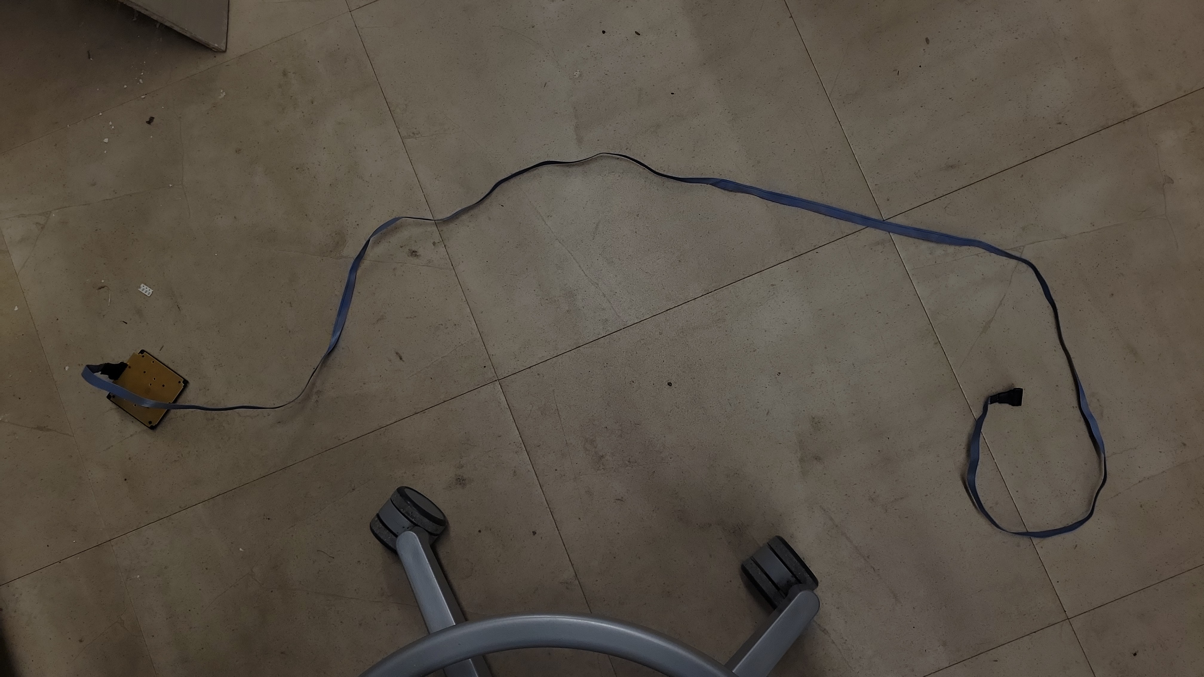
Next I made a cable for our keypad. This took about an hours. It took some time because there are a lot of fiddly wires to solder. I also wanted to make it nice so I used heat shrink and was being careful to have the heat shrink on before I finished soldering. This will be used in our final design. Figure 24 shows this cable. I also spent another hour working on converting the keypad code Jinrea provided to a library we could use, and adding it to our integration code.
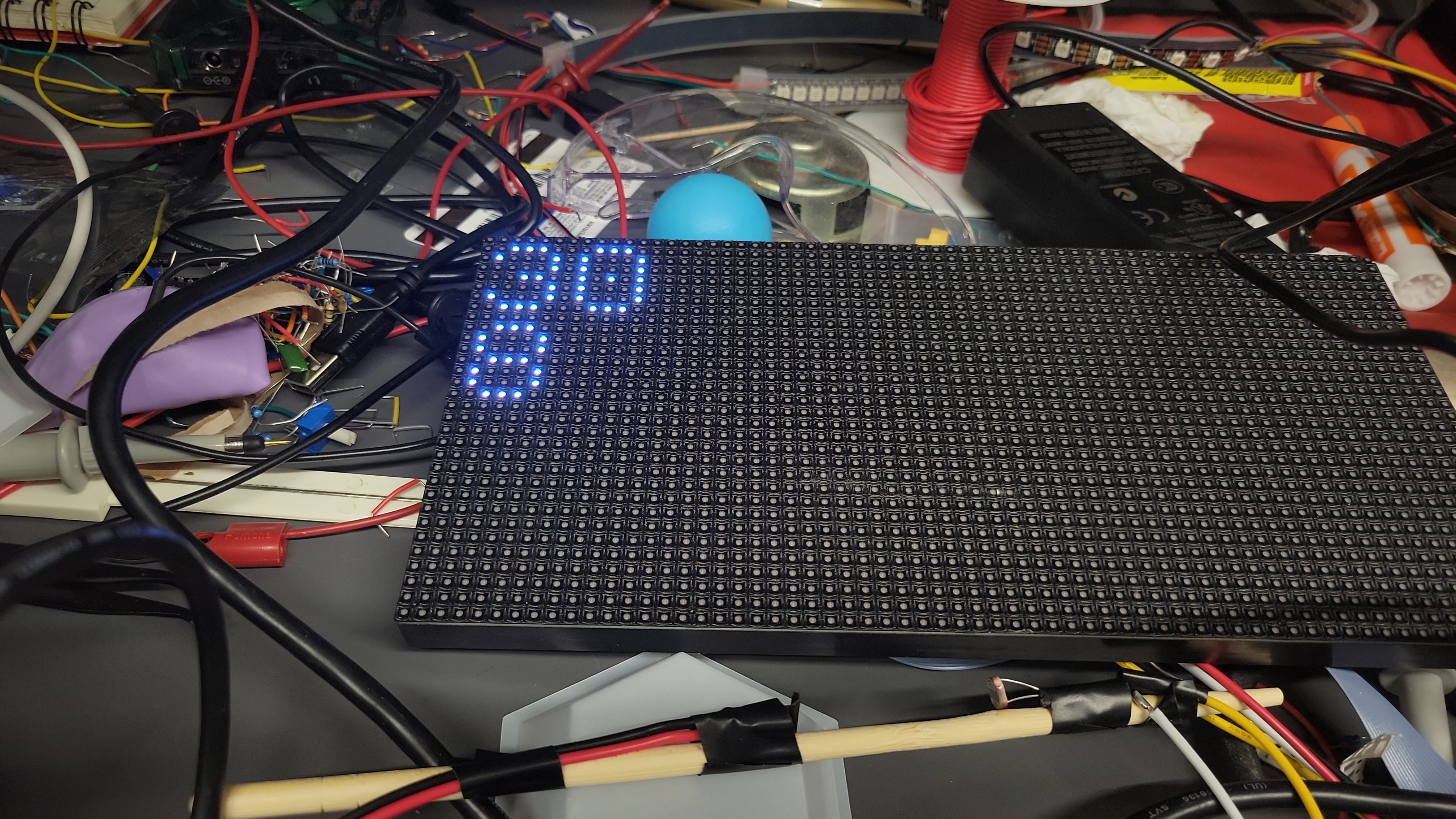
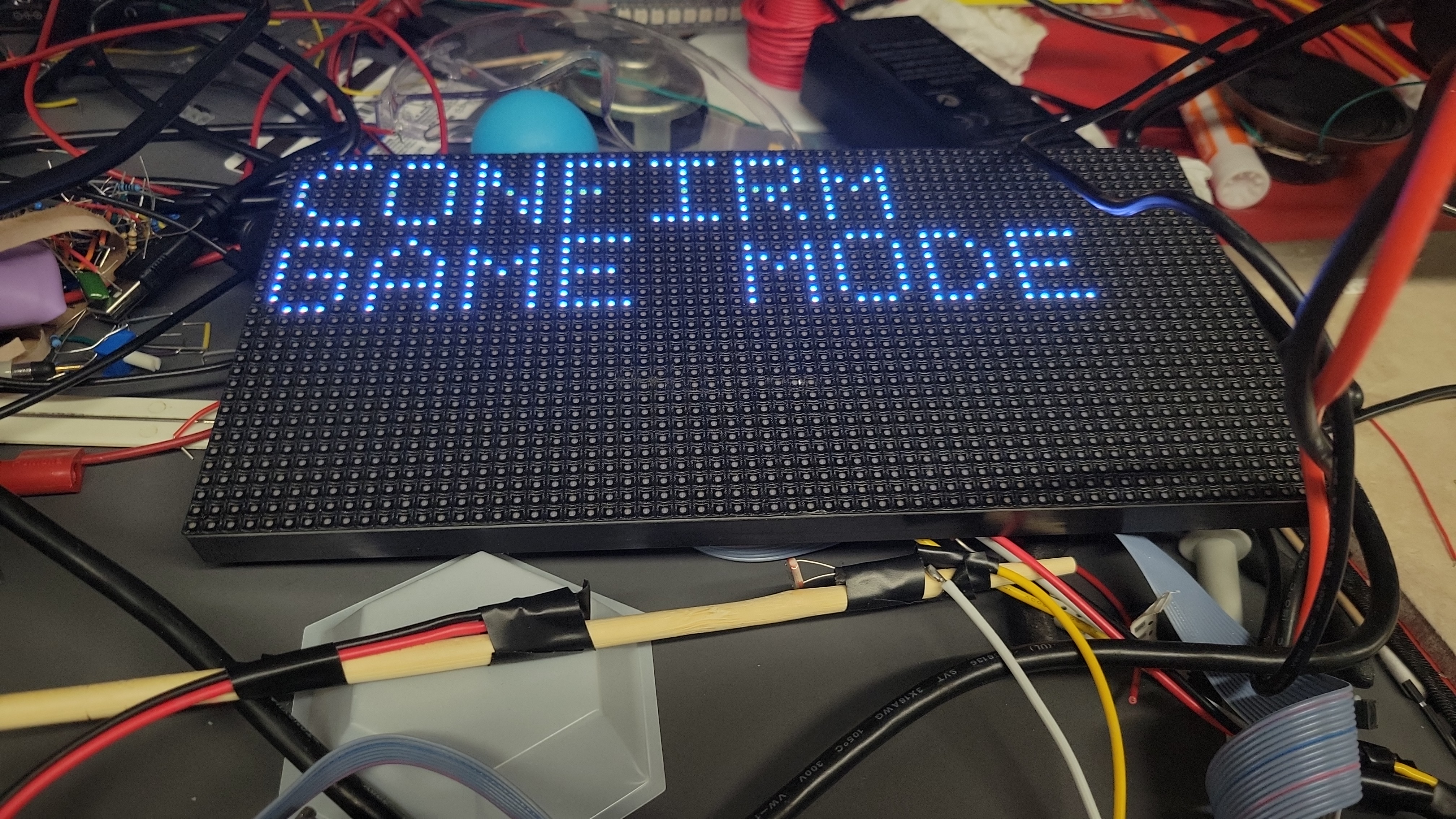
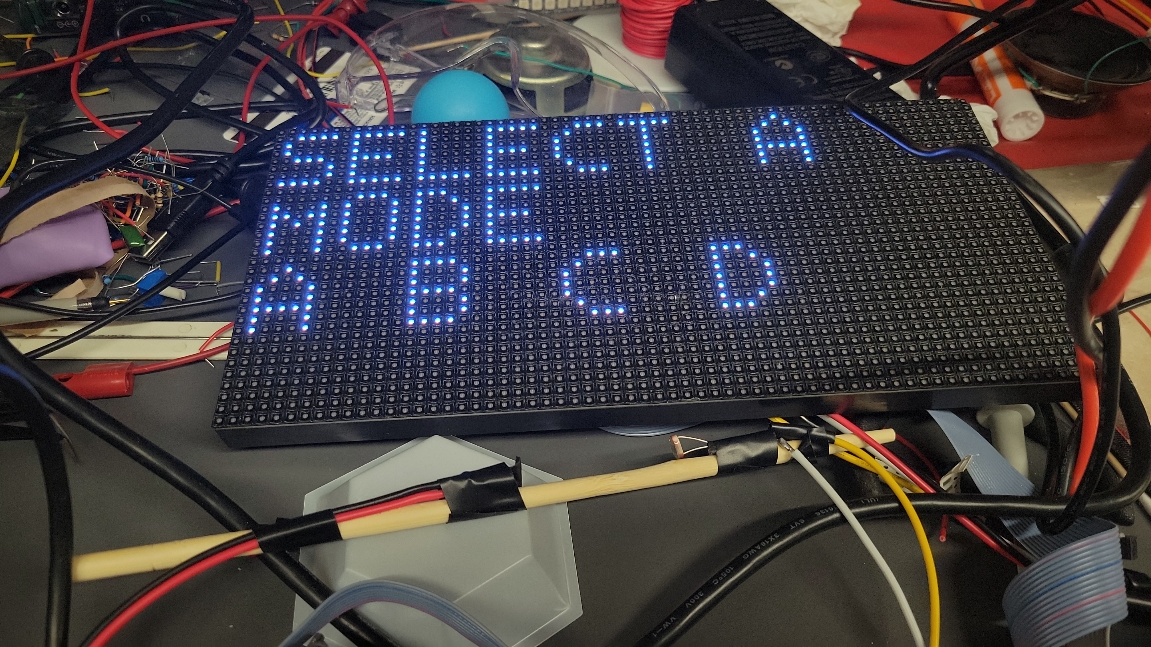
Finally I spent our four hours adding in sensor code and began implementing the game logic. So far I have implemented mode select, time input, the timer, and scoring for Normal, Time Attack and Streak modes. I have not finished Combo mode. Furthermore, the UI elements I am using are very basic and bland, but I am designing the code in such a way that they can be improved at a later time. I also have not started on integrating the audio or the lighting effects with the game logic. This is a very good start to our game logic though, and will be very useful in the future. Figure 25 shows some of the features I have implemented.
Progress Report for Aden Koperczak
WEEK: 11
Date: 11/03/2023Total hours: 94 hours
Project Hours Since Last Report: 17 hours
Cumulative Semester Project Hours: 94 hours
Description of Individual Project Work Efforts: Soldering, Testing on board, Integration of Software, and Packaging Revision.
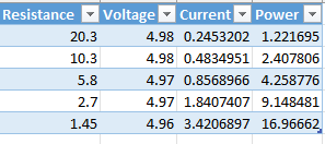
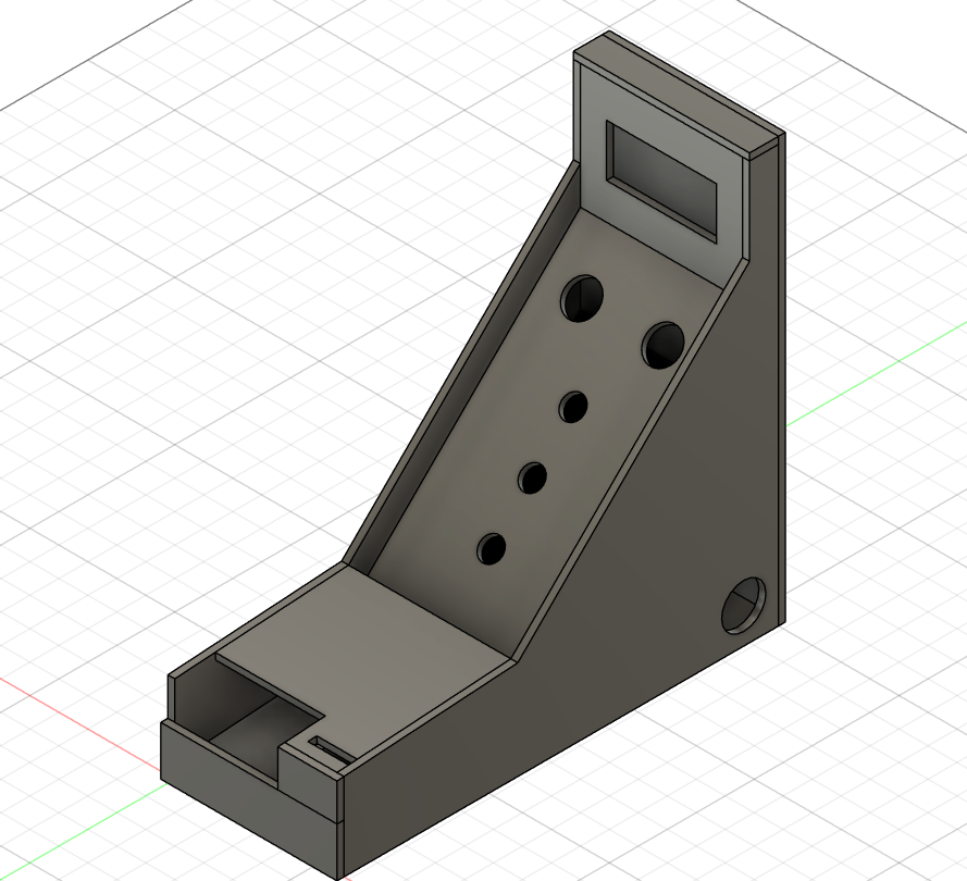
After checking over the circuit board, Eric and I began soldering the buck regulator. I spent around 2 hours working on it before I had to leave and Eric finished it up. The next day I ran a load test on the buck regulator to ensure it was working under load. Figure 22 shows the results. Next Jinrea and I soldered the LDO and had the relevant PSDR singed off on. This took about 2 hours (testing the buck took some time). Then Jinrea and I worked on soldering on the microcontroller. I spent around an 2 hours on it befoer leaving it up to Jinrea to finish. Later I spent around another hour soldering support components and testing the micro with a basic LED flashing program. Then I spent another 3 hours soldering the HUB75 components and trying to get it to properly work. I had a few issues with some imperfect solder joints, the micro needing a slight reflow, some vias having bridged, the 74LS08 not producing high enough voltages, and the chip not being properly seated in its socket. Finally I got that working. I also spent another half our soldering the oscillator, where I had some issues with getting all the needed connections. I spent another half hour testing the audio circuitry Jinrea had soldered. Next I spent around an hour soldering the WS2812B components and testing them. At this point I began integrating our separate programs into one test program to ensure there is no issue with how they interact. This took around another 2 hours. This did reveal some bugs which took an hour to work out (mostly because I was stupid and thought it must be hardware when it was software). Finally, I spent an hour helping Htet solder the sensor hardware. This essentially completed our board. I spent another hour going over the packaging with Jinrea, and we made some modifications (Figure 23).
Progress Report for Aden Koperczak
WEEK: 10
Date: 10/27/2023Total hours: 77 hours
Project Hours Since Last Report: 8 hours
Cumulative Semester Project Hours: 77 hours
Description of Individual Project Work Efforts: Prepared for Soldering, Software planning
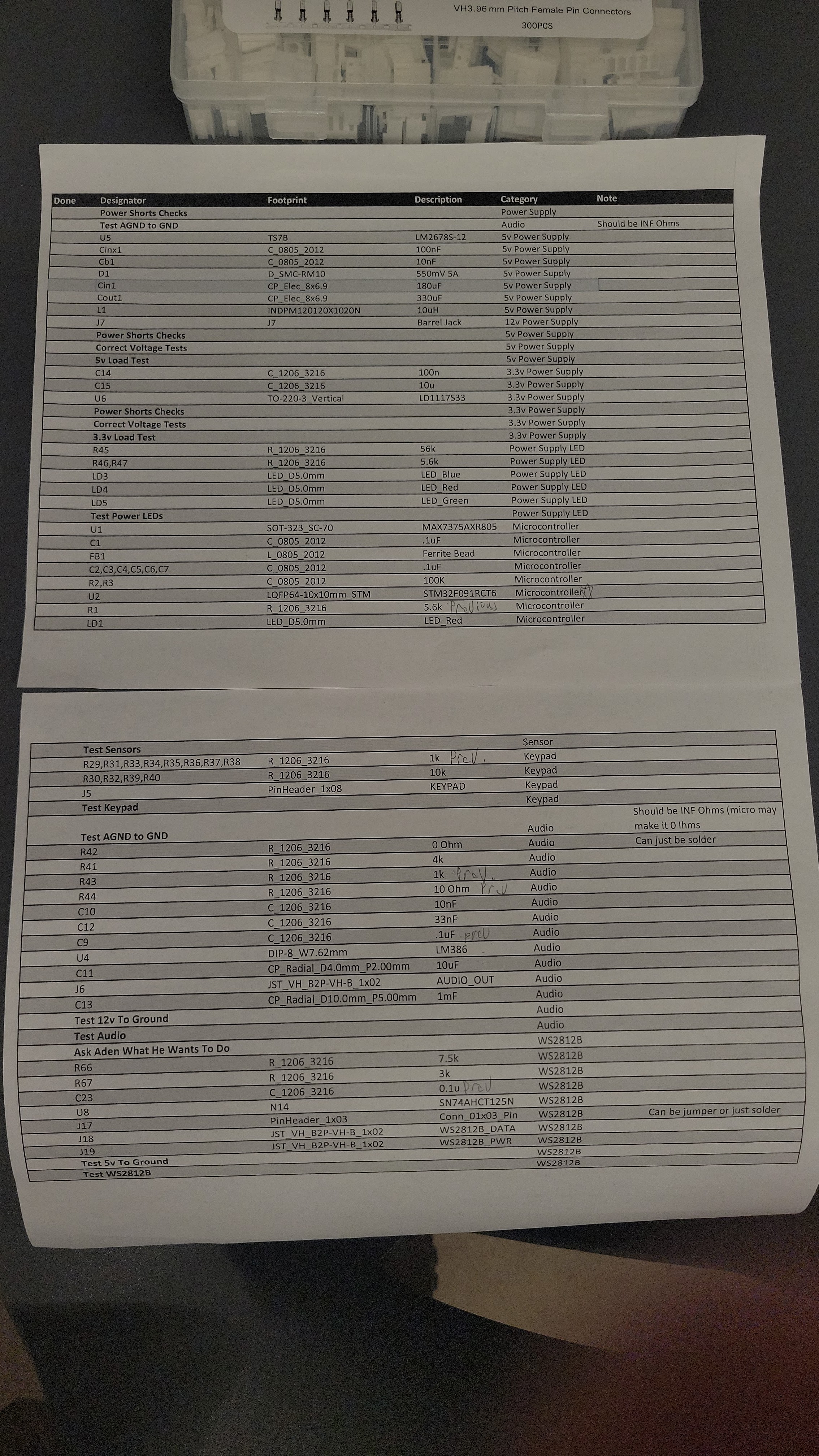
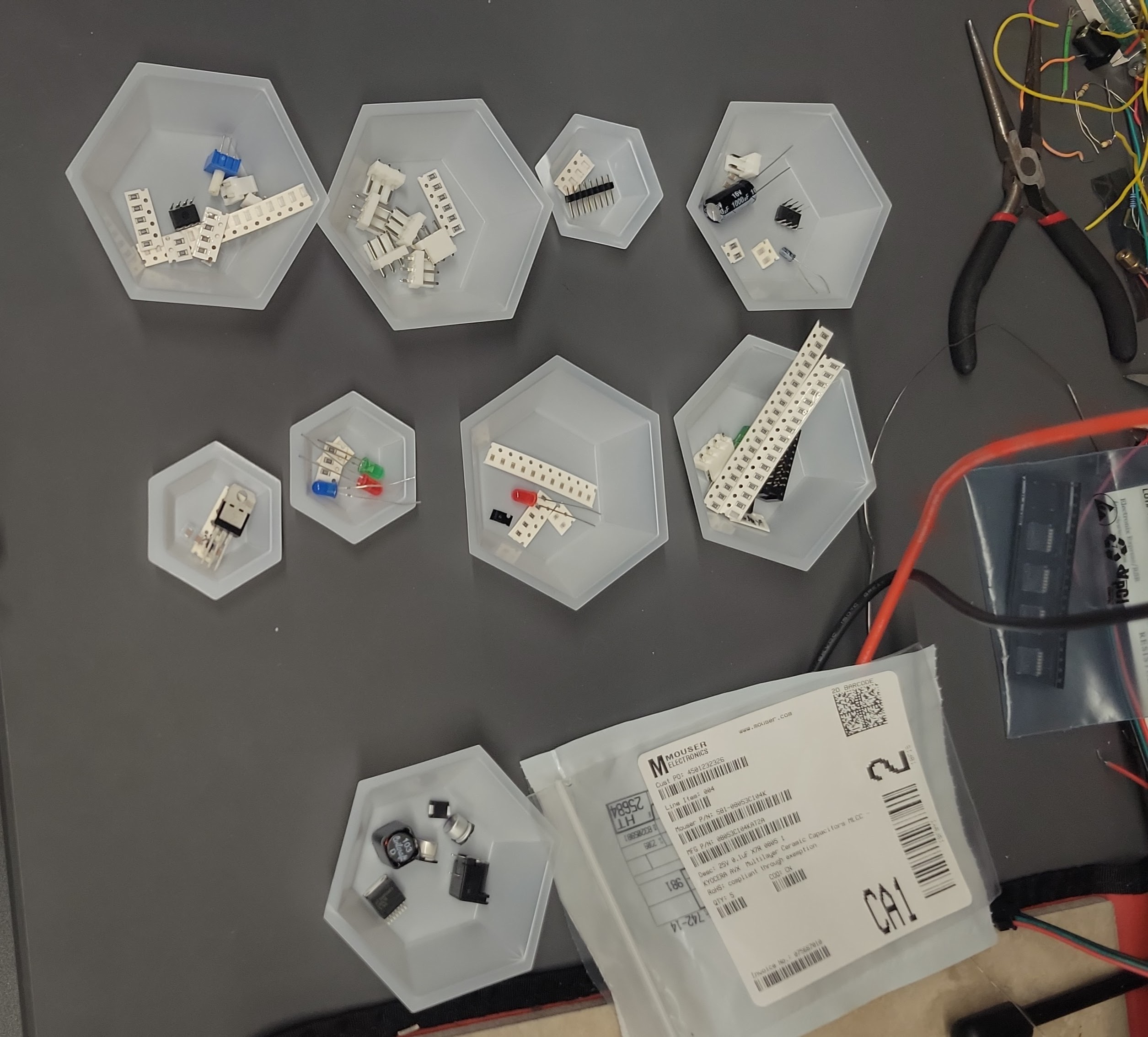
This week I spent most of my time preparing for soldering our board. This consisted of planning the order which we will solder the components in, collecting the components, organizing those components into the order they will be used, and practicing soldering. I spent around 2 hours deciding on an order and making a document with that order on it (Figure 20), about 2 hours collecting components and putting them in order (Figure 21), and around 3 hours practicing soldering. I have soldered SMD components before, and I have been practicing on my own, but it is different using the school's equipment over my own. The solder has less flux than I am use to. I also believe it is lead free whereas I am used to using leaded solder (with good ventilation, there is likely no difference in health effects). Moreover the soldering iron seemed to take longer to heat some of the SMD components than mine does. Finally, I do not have any microscope, let alone a fancy binocular one. I also have an uncommon eye condition which makes my binocular vision imperfect, so having some time to get used to the microscope was useful. All of this work should make soldering our board go more smoothly.
Progress Report for Aden Koperczak
WEEK: 8-9
Date: 10/20/2023Total hours: 71 hours
Project Hours Since Last Report: 13 hours
Cumulative Semester Project Hours: 71 hours
Description of Individual Project Work Efforts: Finnished up Schematic and PCB, Helped Work on Presentation, Worked on Fixes From Presentation.
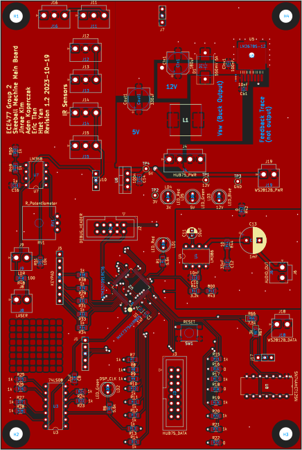
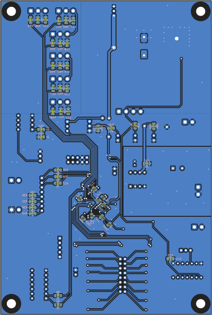
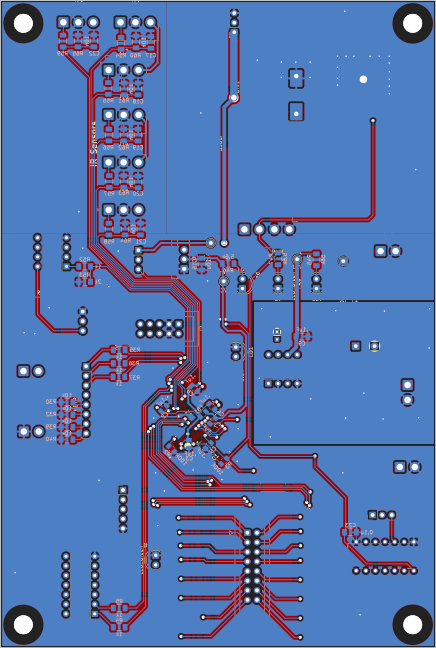
First, I finished up the schematic and the PCB for the midterm presentation. This involved making several minor changes including adding the WS2812B light section to the PCB, modifying the routing around the oscillator, adding the laser circuitry and removing the redundant connectors for the sensors that were replaced by the laser, and adding voltage dividers to the sensors. The routing took the most time because it involved changing around a large number of traces running to the HUB75 display. There were two main issues with the oscillator: it was connected to the wrong pin and it was too far from the pin it needed to connect to. This required rerouting many traces to keep them away from the oscillator. Overall, these modifications took around 6 hours to complete. This allowed us to be ready for our presentation. Figures 17-19 show this progress.
Next, I worked on the presentation. I mostly spent time trying to figure out how to make the different layers easy to see when presented as we would be doing. Everything got very messy, and as soon as you zoomed in on a screen shot, it would get very blurry. I figured out that KiCAD has a way to export the different layers of the PCB as SVG files. I then wrote a Python script to combine these SVG's together in a configurable way. (This script is a bodge. It is not well written, but it works.) I then was able to generate Figures 17-19 with it. I worked with Eric to make sure the colors would work well on the presentation and we added the labels for the individual section of the board. This took around 3 hours in total. This made our presentation far more readable.
Progress Report for Aden Koperczak
WEEK: 7
Date: 10/06/2023Total hours: 61 hours
Project Hours Since Last Report: 14 hours
Cumulative Semester Project Hours: 61 hours
Description of Individual Project Work Efforts: Continued work on Schematic and PCB layout and wrote code for WS2812B lights.
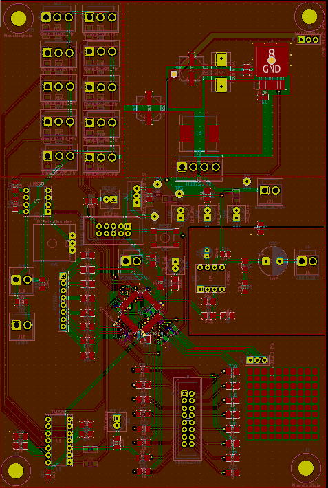
Most of my time this week was spent working on the schematic and PCB layout. I added the sensor connections, the oscillator, and protection resistors to the schematic. I then spent much time routing everything. Because we are using DMA for the HUB75 display, it must use one GPIO port on the microcontroller. In this case, 14 pins are needed. Port A has analog and programming pins, so it cannot be used. Port B has no special pins we need, but the remaining 2 pins would only be useful as input or alternate function pins, which would limit there usability. This leaves port C. Pins 0-13 are free on port C, while 14 and 15 are used for the clock input. (We may only need 14 for our oscillator, but we do not know for sure.) This fits the needed 14 pins in perfectly. This does make routing more complicated because all of the individual ports have their pins spread multiple sides of the microcontroller. Moreover, while having all of the pins for the keypad and the sensors on one port is not necessary, it does make programming for them easier. Those the lower portion of port B is dedicated to the keypad, and the upper section is dedicated to the sensors. This leaves port A for doing the analog output (it is the only port which can do this), debug circuitry and WS2812B lights. The sensor routing is further complicated by the fact that we may need multiple sensors for the gutter of our Skee-Ball machine. Given the active low signal of our sensors, we will need to AND the outputs of the sensors together to get the actual signal. This means we will need to route some of the sensor inputs to the AND gates from the chip we are using for the HUB75 display. While these sensors would work, Htet has also began prototyping a laser break system for the gutter sensor. This could be implemented, or we could simply use multiple sensors to implement this. I also had to import the layout of the power supply that Jinrae and I had previously designed into this new PCB layout. Finally, during this process, Htet, Jinrae, and Eric helped me at varies points. They were useful in finding different routes for wires, verifying footprints, ensuring I did not forget any parts, and in checking pinouts of devices that do not have them pre-made. As I remember, Jinrea helped me with the power supply section, Eric helped me with the audio amplifier and checking the HUB75 connections, and Htet helped me with the sensors and the routing of several signals. This took 11 hours, but some of that time was also spent helping my teammates work, such as checking how well the sensors were working and checking the physical dimensions of the cabinet itself. I would approximate that about 10 hours was spent on the circuit board design and schematic while about an hour was spent helping my teammates. Figure 14 is an image of the most resent PCB layout.
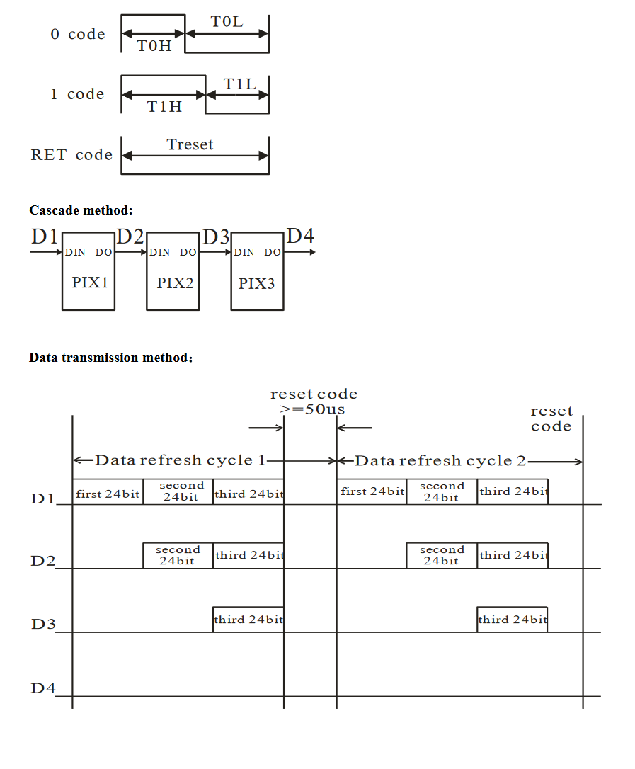
DMA2_Channel2
instead of DMA1_Channel2. Finally, I had completly forgotten that interupts
needed to be enabled through NVIC. Htet asked about this when we were talking about the issue
I was having, and helped me fix that issue. Now we have it working and we have tested it on an
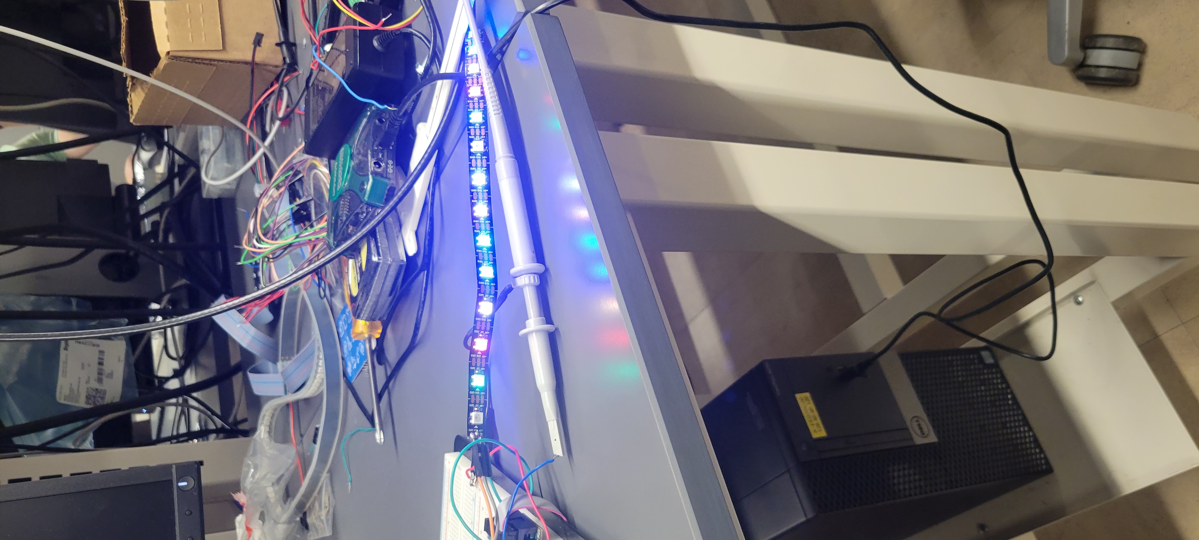
LED strip shown in Figure 16.
Progress Report for Aden Koperczak
WEEK: 6
Date: 09/29/2023Total hours: 47 hours
Project Hours Since Last Report: 8 hours
Cumulative Semester Project Hours: 47 hours
Description of Individual Project Work Efforts: Further work On CAD Model, Work on Power PCB and overall Schematic, Driving Investigated WS2812B
I spent an hour this week tweaking the CAD model, primarily moving the speaker to an external box. This was needed to make the audio more audible.
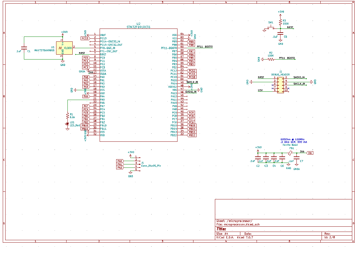
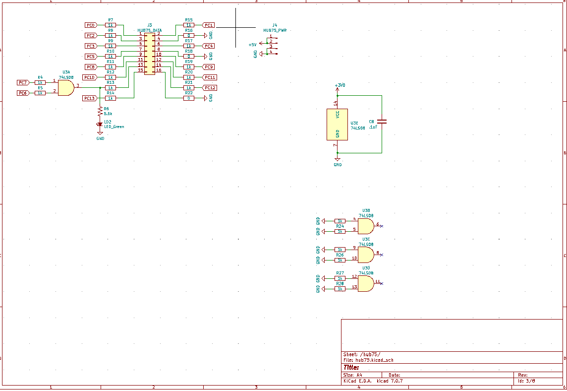
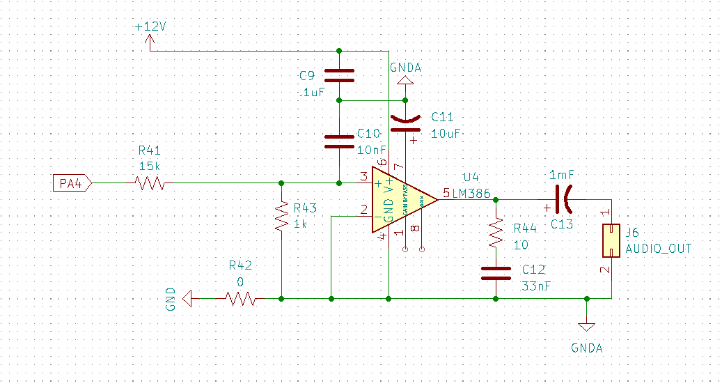
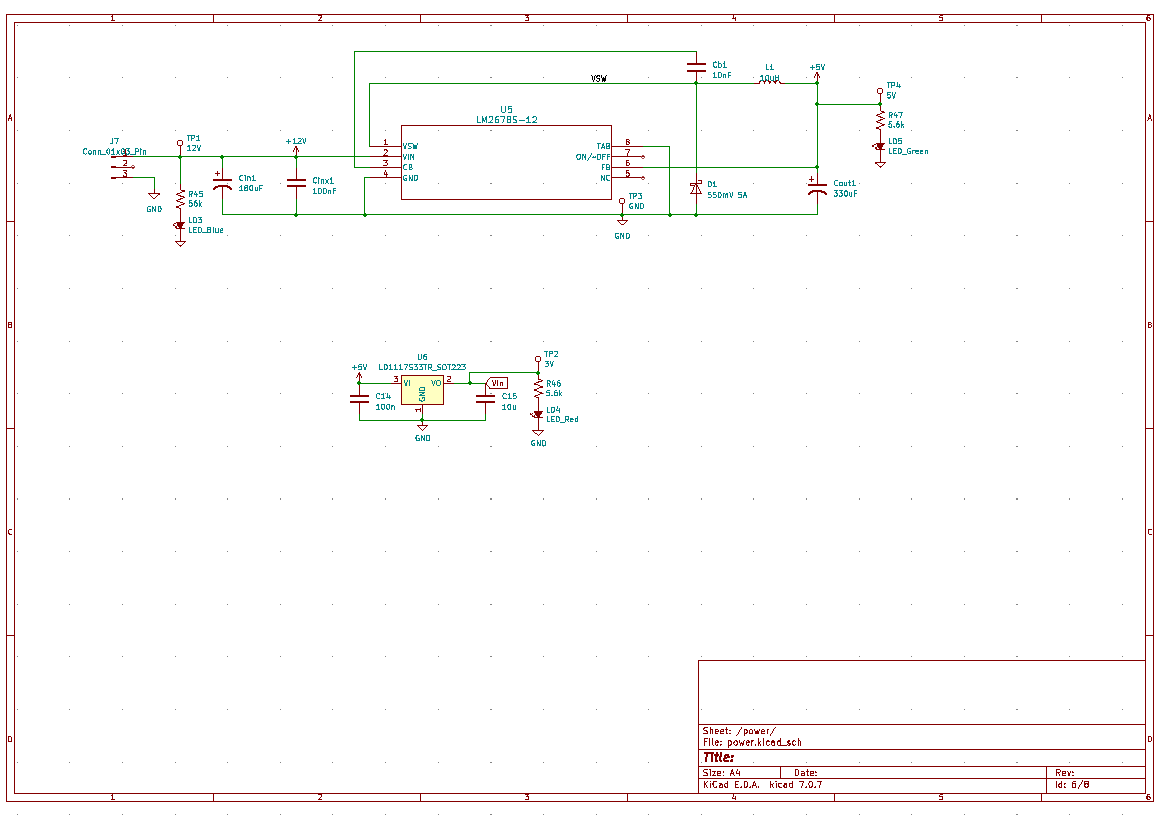
I also spent an hour and a half hours working on making an overall schematic for our design. This is now mostly complete and gives us a starting point for designing the main circuit board for our design. Eric designed the audio circuit, and I pulled some sections from the ECE362 microcontroller development board. Most of this time was taken by finding the symboles for diffrent parts, mainly the microcontroller and the connectors for the display, immporting them correctly, and wiring up the connections correctly. In paticular the display's data connection has many pins that need to be connected correctly in order for it to work.
Progress Report for Aden Koperczak
WEEK: 5
Date: 09/22/2023Total hours: 39 hours
Project Hours Since Last Report: 8 hours
Cumulative Semester Project Hours: 39 hours
Description of Individual Project Work Efforts: Worked on CAD Model, Bought Wood, KiCAD work.
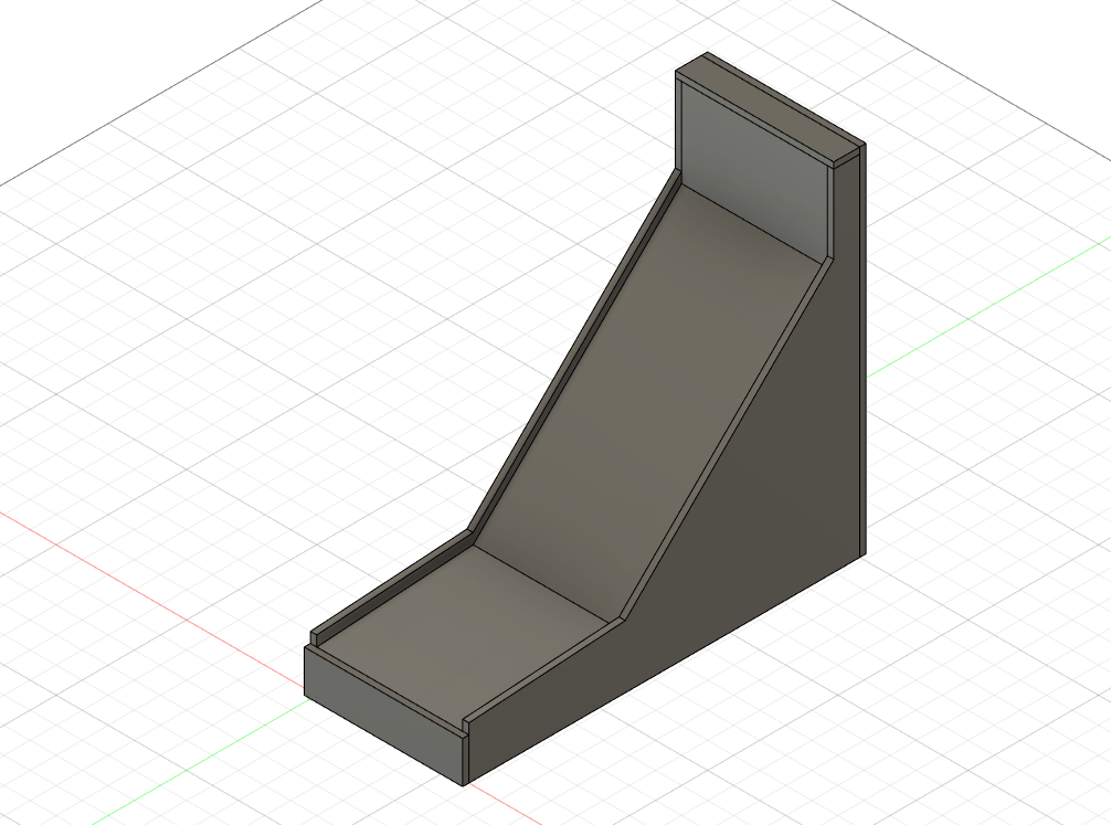
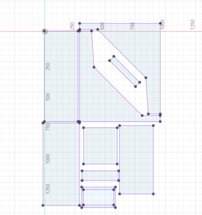
I spent about 6 hours working on the CAD module. My main goals were to make an easy to construct design. We will be cutting basic pieces and laser cutting more complicated parts. Because of this, I was designing with the limitation of laser cutting in mind. We are also using lumber which has imperfect dimensions, so the model cannot rely on the width being correct. I also needed to make sure I did not use any odd dimensions for holes. Finally, I have not made this complex of a CAD model since high school, so it took me more time to do this than if I had more recent practice. Figure 10 shows the model so far. This CAD model can easily be changed in to a rougher path for a laser cutter. I also spent an additional hour picking up the wood from Menards.
Progress Report for Aden Koperczak
WEEK: 4
Date: 09/15/2023Total hours: 31 hours
Project Hours Since Last Report: 8 hours
Cumulative Semester Project Hours: 31 hours
Description of Individual Project Work Efforts: Improve HUB75 display, create first KICAD model, help with choice buck converter, help with amplifier.
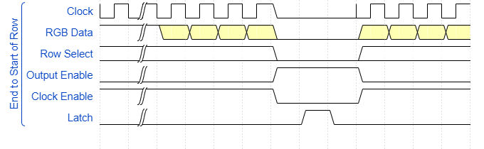
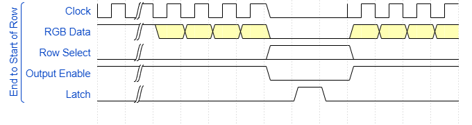
The first thing I worked on this week was improving the HUB75 display. I had misinterpreted the output enable signal as being active positive when it is actually active negative. Eric pointed out my mistake while, so I fixed this. This helped to improve the brightness and stability of the image. Below is the new timing diagram. I also had to add a new "clock enable" line to allow for the shutting off of the clock signal during latching. Figure 6 shows these new signals. This section took about 1 hour to program, modify the circuit, and test this design. This allows us to have a more legible display, especially under strong or outdoor light. It also appears to have improved the stability of the lights, and lower the amount of flicker.
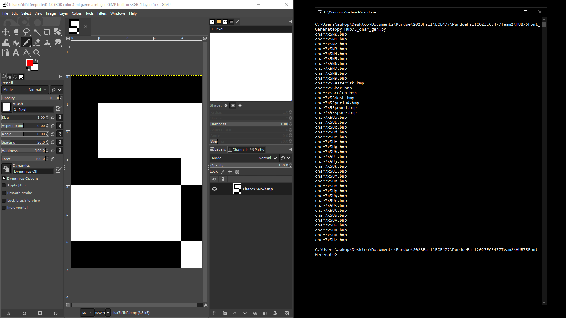
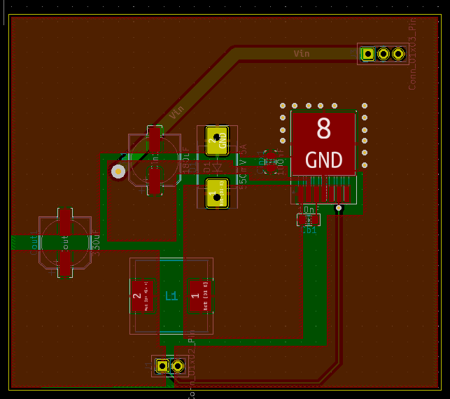
Next, I worked with Jinrae to design a preliminary buck converter circuit board. This was done mostly to give us experience working with KiCAD. The buck converter is the most complicated portion of our circuit board. It is the only section where track placement is supper important. We pulled a design from TIWeBench and the TI datasheet, and created the design in Figure 8. This took us around 3 hours. Although I already had worked with KiCAD, it had been a few years, so I needed some time to refresh my knowledge. I also was showing Jinrae how to do make a design, and letting him work on it. This let us get some experience with KiCad, and should make designing the final board far easier. We also determined that the chip we originally chose was too small to practically solder, so we chose a larger chip.
Progress Report for Aden Koperczak
WEEK: 3
Date: 09/08/2023Total hours: 23 hours
Project Hours Since Last Report: 8 hours
Cumulative Semester Project Hours: 23 hours
Description of Individual Project Work Efforts: Researched, understood, and implemented an interface to a HUB75 64x32 display from the microcontroller.
I spent this week working on the interface to the HUB75 64x32 display. This process consisted of researching the interface, understanding the needed signals, understanding the interfaces available on the microcontroller that could be used to drive the display, and using those interfaces to generate the needed signals.
First I researched the interface, and how it worked. I discovered that the board had 6 sets of shift registers that would hold the color information of two rows at a time. This is combined with some latching LED driver chips which latch the color data for a given row. The latching and output enable of the driver chips is controlled by a latch pin exposed to the interface. Finally a decoder also chooses which rows are powered by the driver chips.
This lead to the general process for the signals that are needed.
- Clock in the parallel color data.
- Disable the clock, output enable, and set the output row selection.
- Pulse the latch output
- Re-enable the clock and output enable
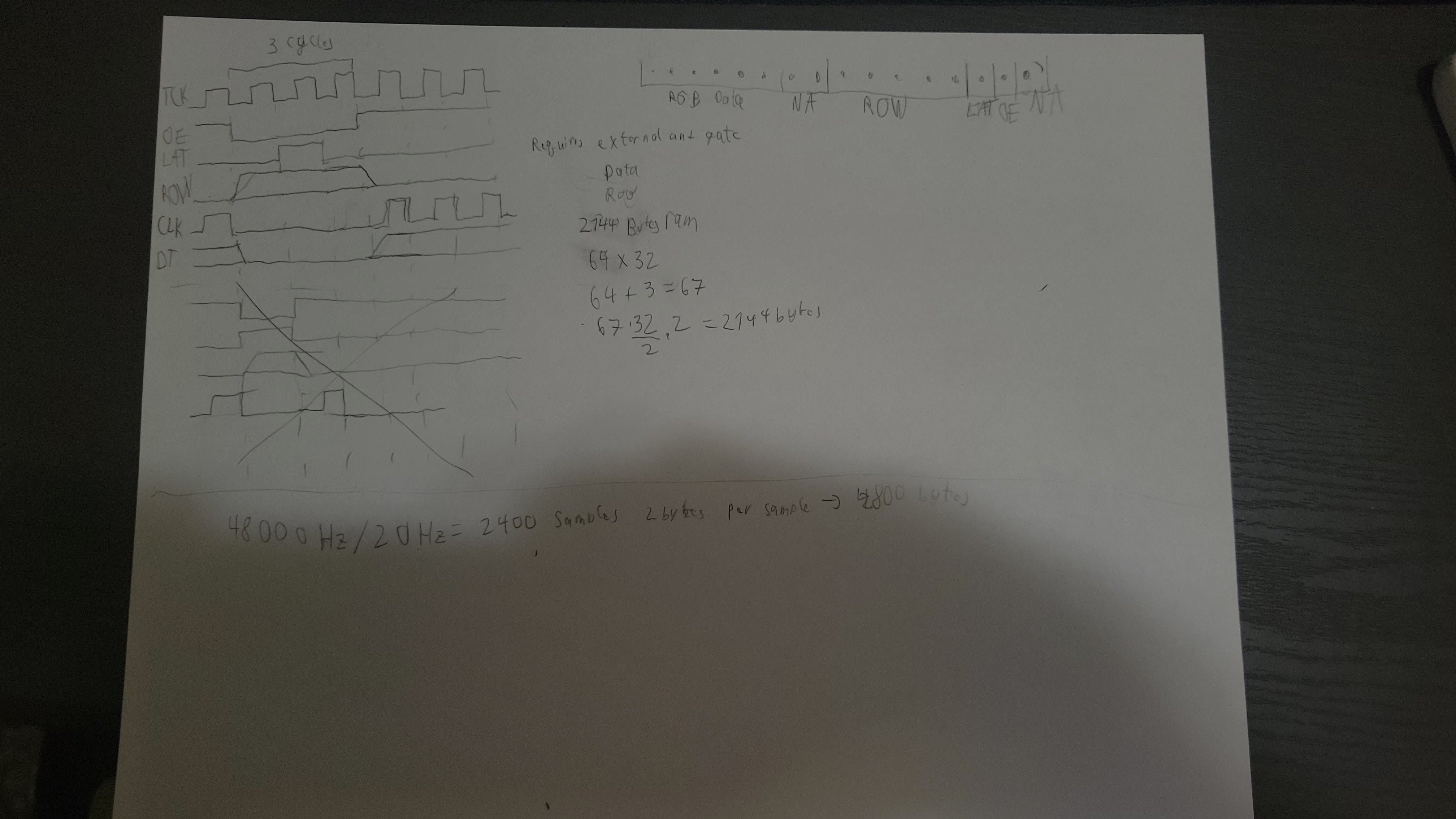
I then looked at what resources on the microcontroller I could use to generate these signals. I decided to use DMA to generate all of the signals except the clock signal, and a timer in PWM mode to generate the clock. The timer also triggers the DMA transfer on the falling edge of the clock. The only problem with this is that the clock signal could not be turned off during the latching phase. To accomplish this I and the clock signal with the output enable signal. The only other option would have required different states for the positive and negative portions of the clock. This would have essentially doubled the memory usage. I then implemented this in code. This took about 2 hours to complete.
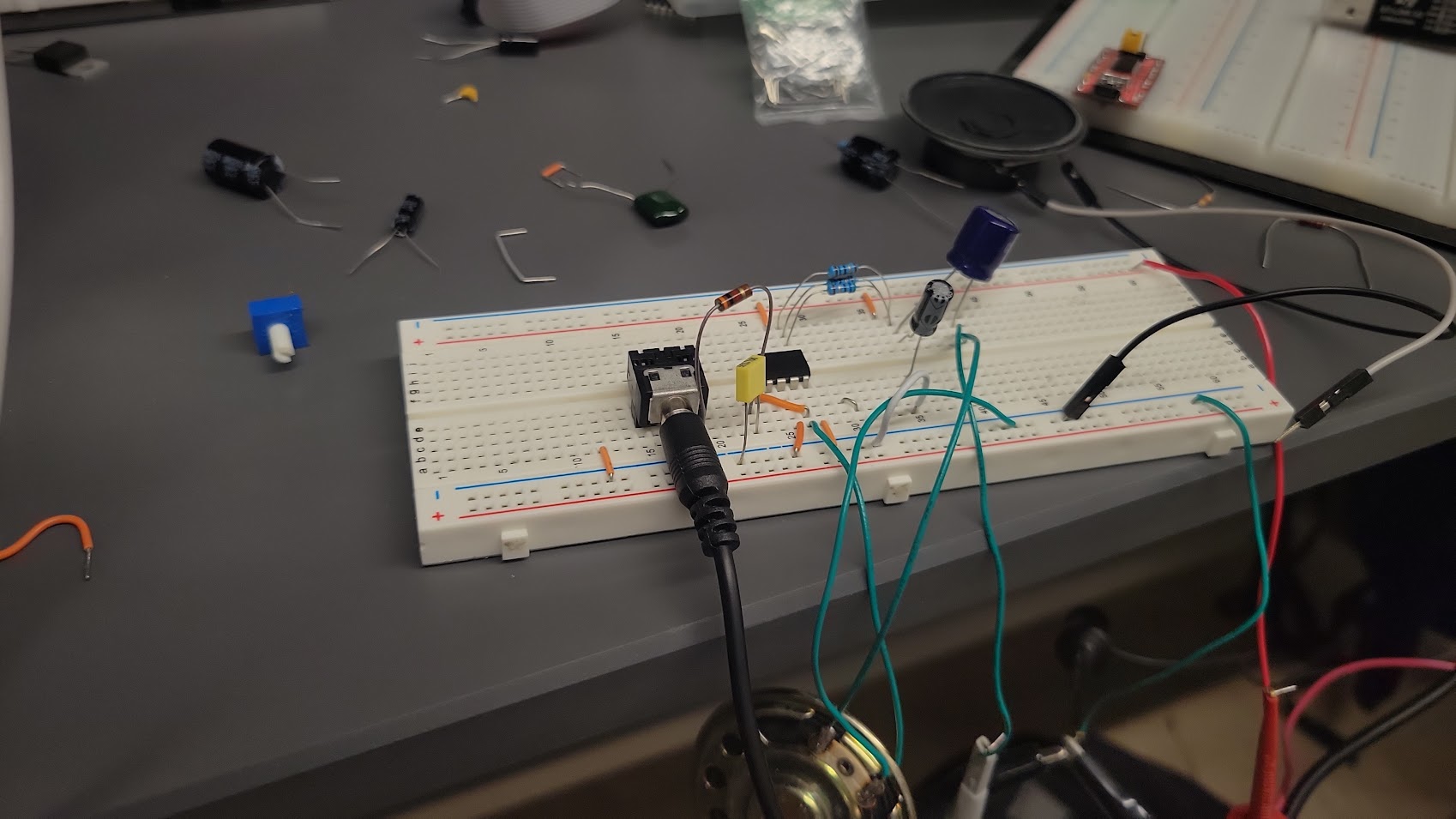
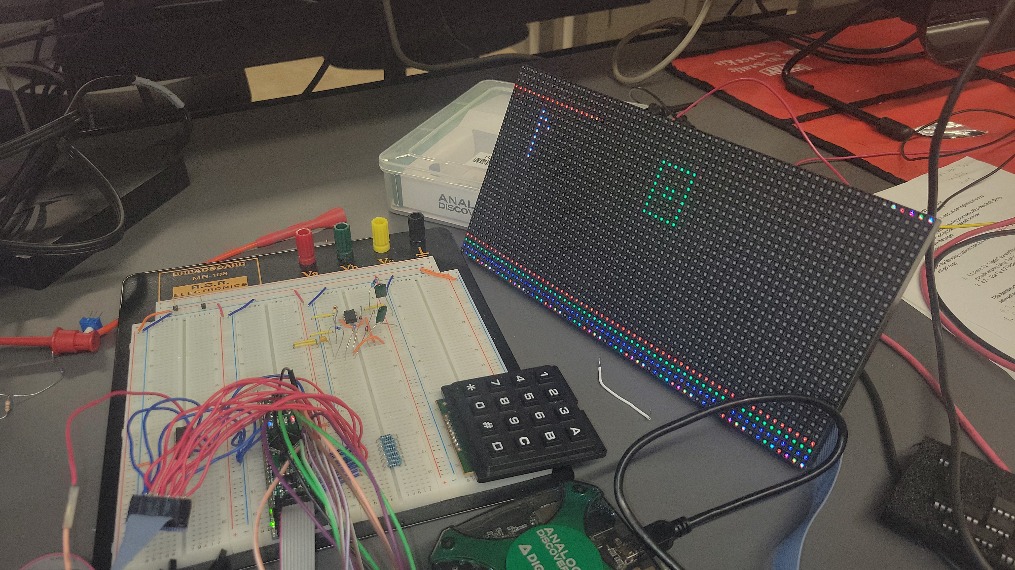
Next I implemented the design on a bread board to test the output. There were some issues with power, understanding the pin out of the connector, and finding a working AND gate. Together this lead to about 2 more hours of work. Finally we had a working prototype as shown in Figure 3, 4, and 5. During this process we also measured the max current the display could draw (Figure 4). This helped us understand our power requirements.
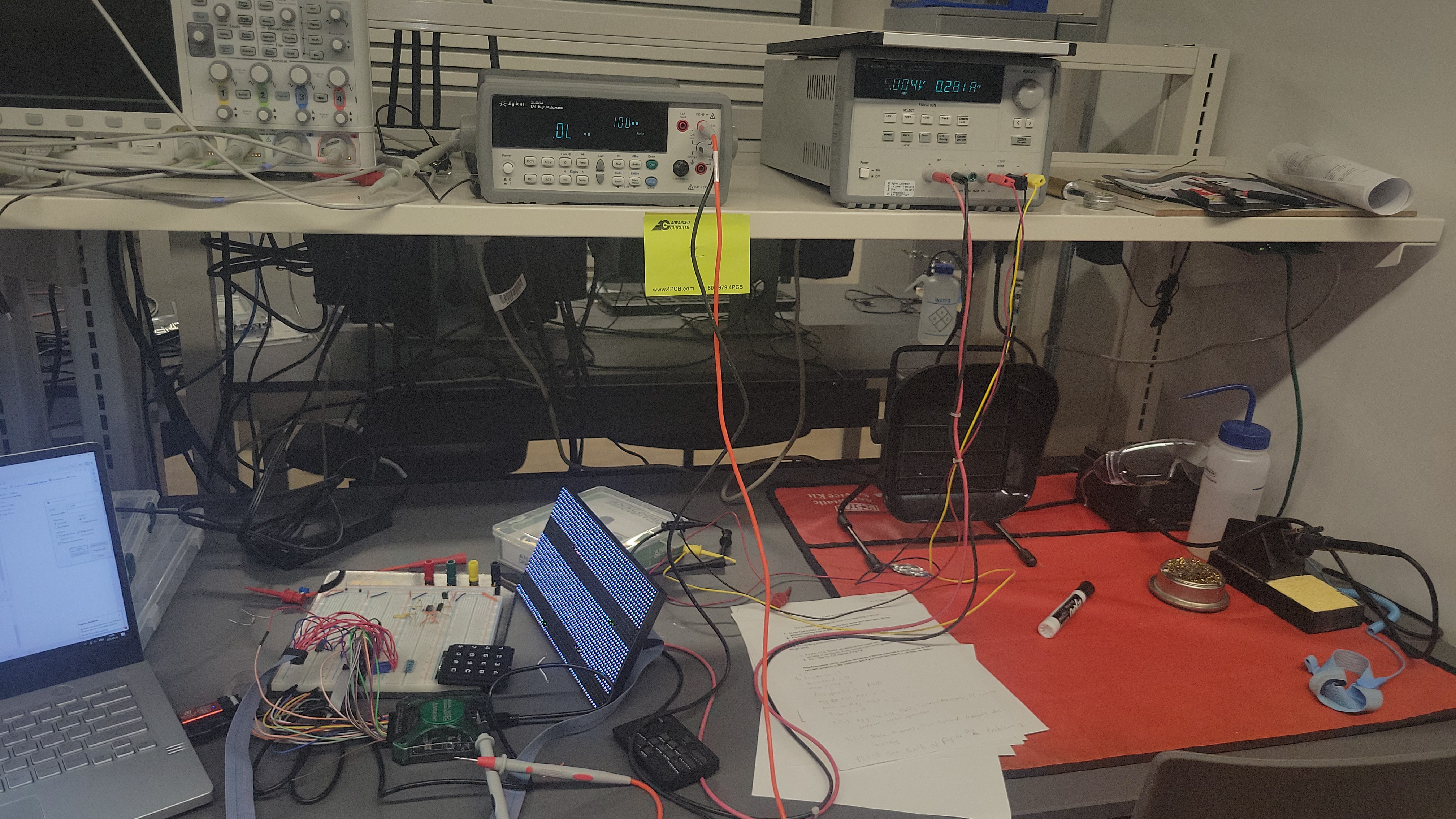
Overall, the creation of this interface is a large section of our PSDR 1. Having completed this we are closer to having a completed project. With this finished we will be able to focus more on other PSDRs and functions.
I also made some suggestions on how to design the buck converter and analog circuity for the speaker. Finally I added all of my code to the GitHub, and documented all of the resources that I used to make the software. This was all done in conjunction with other parts described above, so it did not add any additional time.
Progress Report for Aden Koperczak
WEEK: 1 and 2
Date: 09/01/2023Total hours: 15 hours
Project Hours Since Last Report: 15 hours
Cumulative Semester Project Hours: 15 hours
Description of Individual Project Work Efforts: Set up Website, A0 Market Analysis and General Fixes, A1 Description, Responsibilities and Price
First I worked on the website. Beyond simply copying the web files, I also made the website be in a dark mode by modifying "css/default.css" and "css/style.css", added contact information, and helped guide my teammates on how to set up their portions of the website. I used a mapped drive on Windows to access the website, and GVim as an editor to modify the HTML and CSS files I needed to modify. This helps to advertise our work, and show our progress. I learned some about how this particular website was set up and had the chance to practice HTML and CSS. I will continue to work to keep the website up to date, and ensure there are no issues with the styling of the website.
I also rewrote the Market Analysis section of A0 to make use of more sources and statistics. I also helped make general fixes such as adding source numbers to the Open Source Products section. I used Word and OneDrive to edit the A0 document. I also used CitationMachine to check my citations. This helped me understand the potential market for our device, and gives us incite into what people are looking for in the market.
For A1 I wrote an initial description which was added to by others, helped make the Responsibilities, and made an initial price estimate, which was modified as we chose more specific ideas on what we would be using. I used Word and OneDrive to edit the A1 document. This allows us to understand what our projects goals are and what parts we need, and gave us an estimate of how much we will be spending in total for this project.